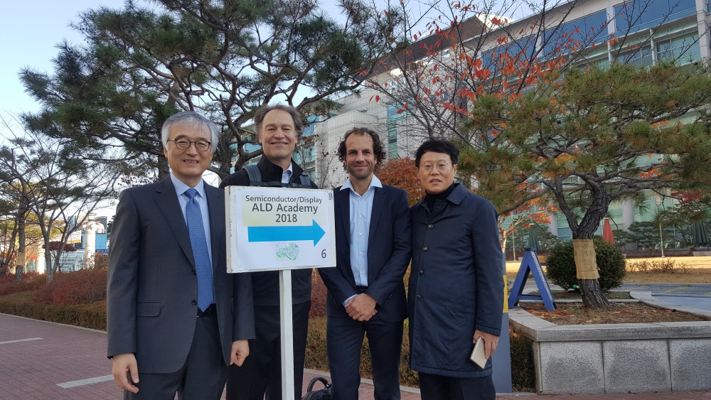
This course was given on 12 November 2018 at Hanyang University in Seoul, Korea. It was organized through The Korean Society of Semiconductor & Display Technology (KSDT) by prof. Hyeongtag Jeon. The speakers were prof. Gregory Parsons and prof. Erwin Kessels. The number of attendants was well over 100.
The course covered ALD basics (especially the underlying surface chemistry) as well as advanced ALD processes (including plasma-enhanced ALD and spatial ALD). The ALD processes addressed weremainly be related to applications relevant for the semiconductor and display industry.
Furthermore, recent developments in the field of atomic scale processing were discussed. This includes area-selective deposition (ASD) and atomic layer etching (ALE).
Responses to the course:
Professionals(<5 years) Professionals(>5 years) Students Postdocs32 34.8% 29 31.5% 27 29.3% 4 4.3%
4.5 out of 5.0 stars The course was well presented by the speakers
4.3 out of 5.0 stars The course met my expectations
4.3 out of 5.0 stars The course provided useful skills
4.3 out of 5.0 stars The course was well setup
4.3 out of 5.0 starsI would recommend the course to others
Schedule:
| 09:00-09:10 | Greeting | Prof. Park (KSDT) |
| 09:10-09:20 | Introduction ALD Academy | Parsons, Kessels |
| 09:10-10:00 | Lecture preview | Parsons, Kessels |
| 10:00-10:50 | ALD basics I Surface chemistry | Kessels |
| 10:50-11:10 | Morning break | |
| 11:10-12:00 | ALD basics II Precursors | Parsons |
| 12:00-13:30 | Lunch break | |
| 13:30-14:20 | Advanced ALD processes I Plasma ALD | Kessels |
| 14:20-15:10 | Advanced ALD processes II Spatial ALD | Parsons |
| 15:10-15:30 | Afternoon break | |
| 15:30-16:20 | Atomic scale processing I Atomic layer etching | Kessels |
| 16:20-17:10 | Atomic scale processing II Area-selective deposition | Parsons |
| 17:10-17:30 | Wrap up & closing | Parsons, Kessels |
For additional information, please contact:
Prof. Hyeongtag Jeon
Division of Materials Science and Engineering
Hanyang University
Email address: hjeon@hanyang.ac.kr